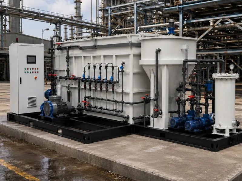
Semiconductor manufacturing generates substantial volumes of wastewater containing dissolved salts, metals, organic compounds, and suspended solids that demand rigorous treatment before discharge or reuse. Semiconductor wastewater treatment requires a dual approach that integrates effective pretreatment processes with comprehensive water reuse strategies to minimize environmental impact and operational costs. This combined methodology transforms wastewater from a liability into a recoverable resource, supporting both regulatory compliance and facility sustainability goals.
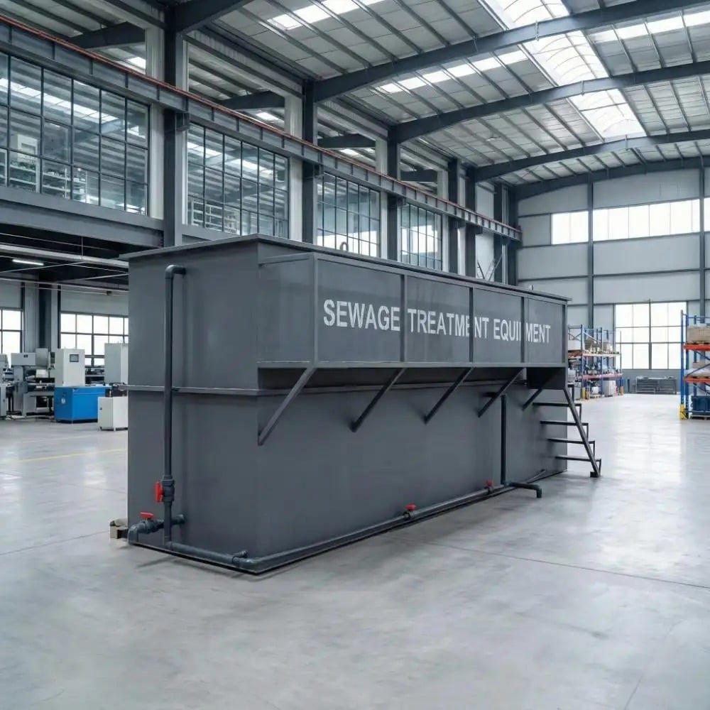
The integration of pretreatment and reuse represents a fundamental shift in how semiconductor facilities manage water resources. By implementing strategic pretreatment stages upstream, facilities can condition wastewater to quality levels suitable for reuse in cooling systems, process water, or facility operations. This integrated approach reduces freshwater consumption, lowers discharge volumes, and creates long-term operational resilience while maintaining compliance with increasingly stringent environmental regulations across semiconductor manufacturing regions.
Understanding Pretreatment in Semiconductor Wastewater Management
Core Pretreatment Objectives and Methods
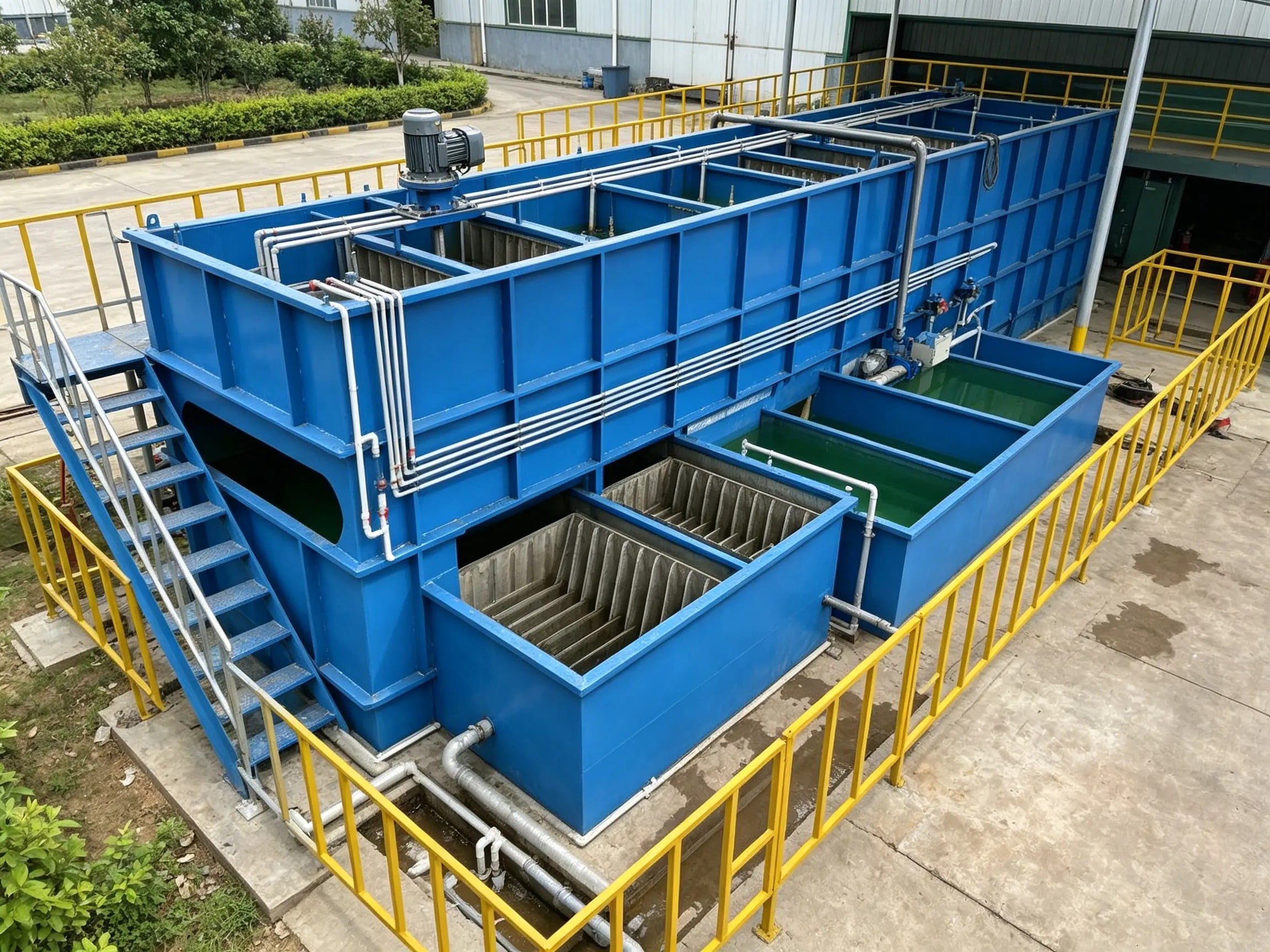
Effective pretreatment removes particulates, dissolved ions, and contaminants that would otherwise interfere with advanced treatment stages or reuse applications. Semiconductor pretreatment typically begins with coagulation and flocculation to aggregate suspended solids, followed by sedimentation or clarification to separate solids from the liquid stream. Chemical precipitation removes dissolved metals and phosphates, while pH adjustment ensures optimal conditions for subsequent treatment stages.
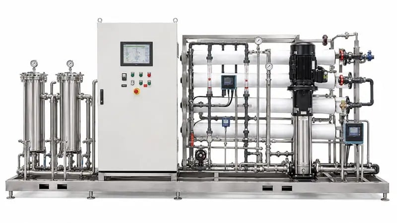
Membrane-based pretreatment systems have become essential in semiconductor operations. Microfiltration and ultrafiltration units remove particles down to the micron level, preparing water for membrane technologies that achieve the stringent purity requirements semiconductor processes demand. These pretreatment stages reduce fouling of downstream equipment, extend membrane lifespan, and improve overall treatment efficiency.
Pretreatment Integration with Advanced Treatment
Pretreatment success depends on understanding downstream requirements and designing removal sequences accordingly. A membrane system receiving poorly pretreated water faces accelerated fouling and shortened operational cycles, increasing maintenance costs and reducing water recovery rates. Semiconductor facilities that invest in robust pretreatment infrastructure achieve superior membrane performance, lower total treatment costs, and greater flexibility in reuse applications.
Monitoring pretreatment effectiveness through turbidity measurement, particle size analysis, and conductivity tracking enables real-time optimization. Semiconductor operators who establish clear pretreatment performance metrics can adjust chemical dosing, retention times, and flow rates to maintain consistent quality feeding into advanced treatment stages.
Water Reuse Strategies in Semiconductor Operations
Identifying Suitable Reuse Applications
Semiconductor wastewater treatment becomes economically viable when treated effluent meets established quality standards for specific reuse applications. Cooling tower makeup water typically tolerates higher dissolved solids concentrations than process water for cleaning or rinse applications. Facility personnel must first map potential reuse points, establish quality requirements for each application, and design treatment pathways that achieve those targets cost-effectively.
Reuse economics improve when facilities treat wastewater to intermediate quality levels rather than pursuing maximum purity for all applications. A semiconductor pretreatment system might produce water suitable for cooling applications while a second membrane stage achieves higher purity for process reuse. This tiered approach optimizes capital investment and minimizes energy consumption compared to polishing all wastewater to the highest standard.
Implementing Effective Reuse Systems
Successful reuse requires storage capacity, distribution infrastructure, and quality assurance monitoring to ensure treated water consistently meets application specifications. Semiconductor facilities implementing reuse systems typically establish storage tanks sized to buffer daily flow variations, with segregated distribution lines to prevent cross-contamination. Regular sampling and analysis of reused water confirm that treatment processes maintain required quality despite seasonal variations or process changes.
Risk management becomes critical when reusing treated wastewater. Semiconductor operations must establish contingency protocols ensuring that temporary treatment upsets do not compromise facility processes or product quality. Backup freshwater connections, alert systems monitoring reuse water quality, and trained personnel response procedures protect operations while maximizing reuse benefits.
Integrating Pretreatment and Reuse for Optimal Performance
System Design and Operational Synergies
Combining pretreatment and reuse strategies creates operational synergies that exceed the benefits of either approach alone. Semiconductor facilities designing integrated systems must ensure pretreatment stages produce water quality matching reuse application requirements while maintaining sufficient recovery rates for economic viability. The membrane systems used in pretreatment directly influence reuse water quality, downstream maintenance requirements, and long-term operational costs.
A well-designed semiconductor wastewater treatment system views pretreatment not as a standalone stage but as preparation enabling reliable reuse. This perspective drives material selection, equipment sizing, and process control decisions throughout the treatment train. Facilities that optimize this integration achieve higher water recovery rates, lower per-gallon treatment costs, and greater operational flexibility than those treating wastewater in isolated stages.
Monitoring, Optimization, and Continuous Improvement
Integrated pretreatment and reuse systems require comprehensive monitoring to identify optimization opportunities and prevent operational failures. Semiconductor operators should track parameters including flowrate recovery, pollutant removal efficiency, membrane pressure differentials, and reuse water quality metrics. This data reveals seasonal patterns, equipment aging effects, and process variations enabling continuous system refinement.
Capital and operational cost reductions emerge when semiconductor facilities systematically optimize integrated treatment systems. Process improvements might include adjusted pretreatment chemical dosing, modified membrane operating pressures, or reuse routing changes that enhance overall recovery or reduce energy consumption. Facilities committed to monitoring and continuous improvement extract maximum economic and environmental value from wastewater treatment investments.
FAQ
What specific contaminants require removal in semiconductor wastewater treatment?
Semiconductor wastewater treatment must address dissolved metals including copper, tungsten, and tantalum; fluoride from etching processes; organic compounds; suspended particles; and salts from rinse and cleaning operations. Each contaminant demands targeted removal methods, with pretreatment typically addressing particles and metals while membrane systems remove dissolved ions and fine organics. The specific contaminant profile varies by semiconductor process type and manufacturing location, requiring facilities to analyze their wastewater composition before designing treatment systems.
How much water can semiconductor facilities realistically reuse through integrated treatment?
Semiconductor facilities implementing comprehensive pretreatment and reuse systems typically recover 40 to 70 percent of wastewater for non-process applications, with some operations achieving higher recovery through advanced membrane technology and careful process management. Recovery percentages depend on wastewater volume, quality requirements for reuse applications, and membrane system design. Facilities focusing reuse on cooling tower makeup and facility cleaning rather than stringent process applications maximize recovery rates and economic returns.
What is the typical payback period for integrated semiconductor wastewater treatment systems?
Integrated pretreatment and reuse systems typically achieve payback periods of three to seven years depending on facility water costs, wastewater volume, treatment complexity, and available incentives or regulatory credits. High-water-cost regions and facilities with substantial wastewater volumes experience faster payback as the value of recovered water increases. Beyond financial returns, integrated systems provide operational resilience through reduced freshwater dependence and regulatory advantages through demonstrated environmental stewardship in semiconductor manufacturing.

 EN