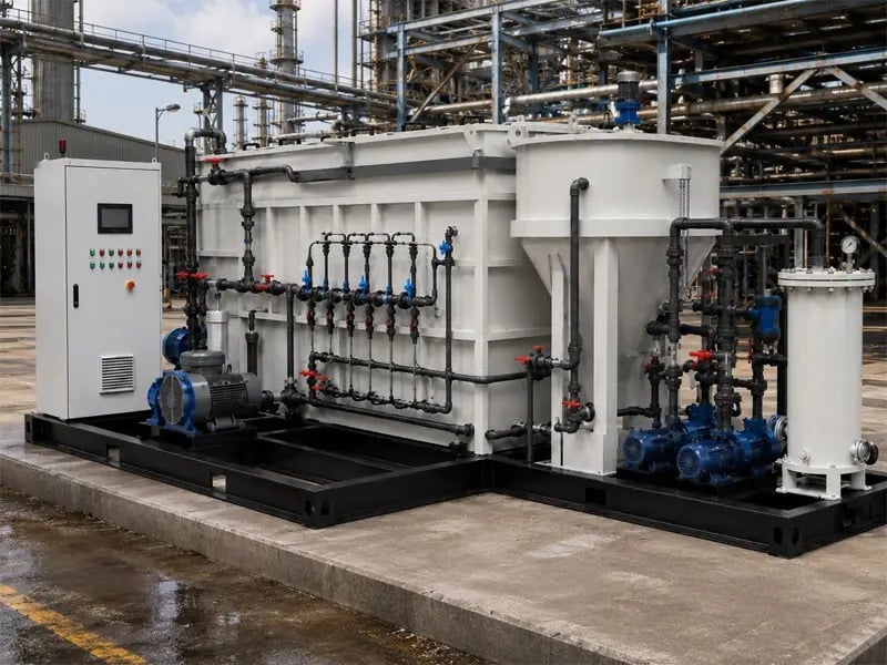
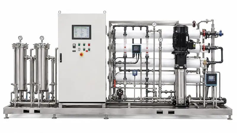
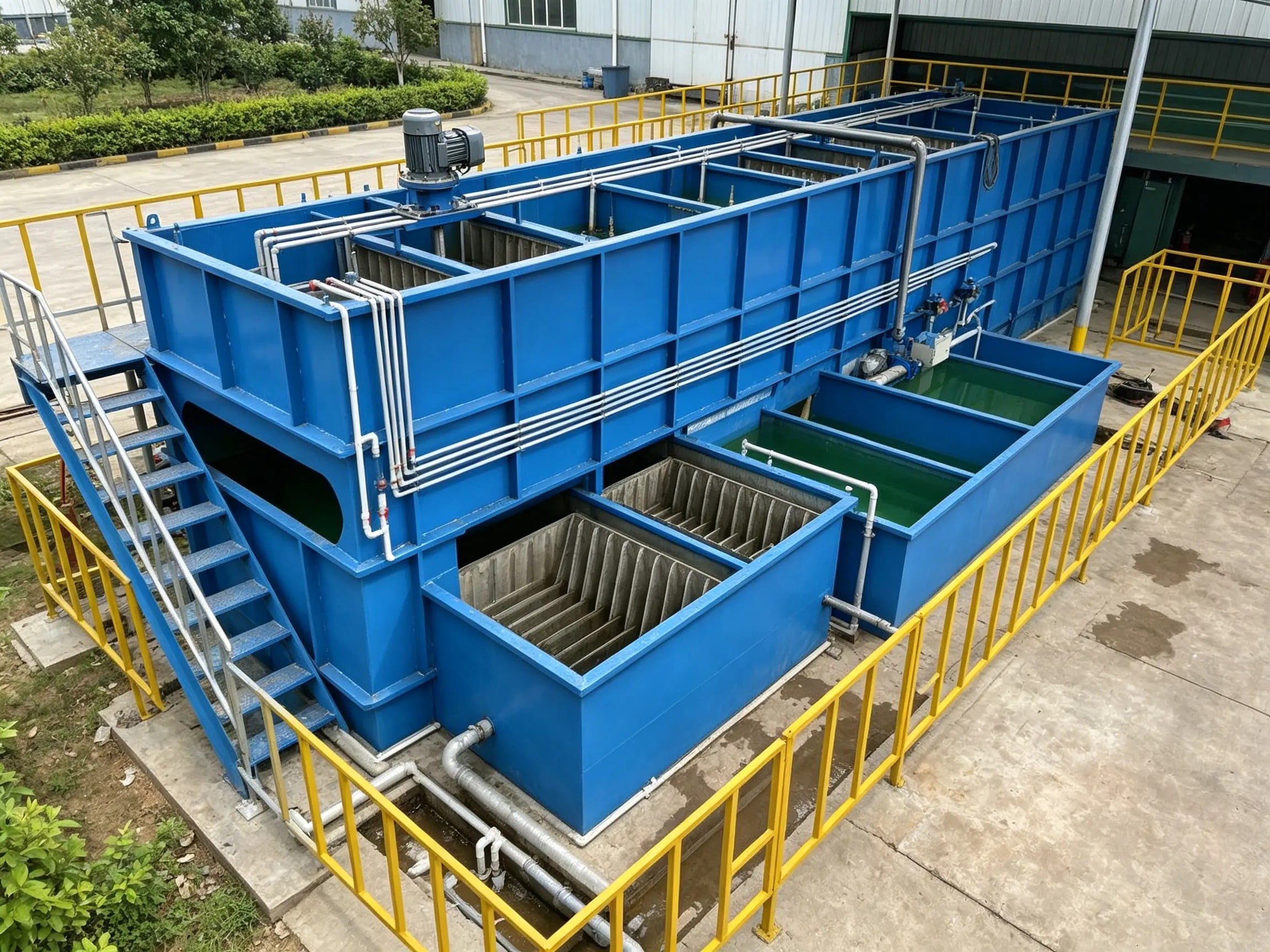
Building a water balance for a semiconductor wastewater treatment plant requires systematic planning, accurate measurement, and strategic flow optimization. A water balance serves as the foundation for understanding how water moves through your treatment facility, where losses occur, and where reuse opportunities exist. Without a clear picture of your water movements, you cannot effectively minimize waste, reduce operational costs, or meet regulatory compliance standards. The process involves mapping all incoming and outgoing streams, identifying treatment pathways, and quantifying each stage to create a complete water accounting system.
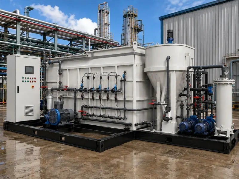
A properly constructed water balance enables semiconductor manufacturers to achieve three critical goals: reducing freshwater intake, maximizing wastewater reuse, and ensuring consistent treatment performance. In semiconductor fabrication, water is essential for cooling, cleaning, and chemical processes, but managing the resulting wastewater streams presents significant complexity. By implementing a detailed water balance framework, your facility gains transparency over volumetric flow rates, discharge volumes, and reuse potential across all treatment pathways.
Understanding Your Incoming and Outgoing Water Streams
Categorizing Source Water and Process Flows
The first step in building a water balance is accurately identifying and measuring all water entering your semiconductor wastewater treatment plant. Incoming flows typically include process water from fab operations, cooling water from equipment, rinsing water from manufacturing stages, and auxiliary water for support functions. Each source carries different contaminant profiles and treatment requirements. Understanding the volume and characteristics of each stream enables you to design appropriate treatment pathways. Document the seasonal variations, peak flow rates, and minimum flow rates for each source to account for operational fluctuations.
Outgoing water streams from your semiconductor wastewater treatment plant include treated effluent for discharge, water sent for reuse applications, evaporative losses, and reject streams from treatment processes. Accurately measuring each outgoing stream is essential for water balance closure and identifying recovery opportunities. Advanced meters and monitoring systems provide real-time data on flow volumes, allowing you to detect anomalies and optimize treatment sequences.
Tracking Treatment Process Losses
Water losses occur throughout treatment operations in a semiconductor wastewater treatment plant through evaporation, sludge dewatering, and membrane rejection during advanced treatment stages. These losses represent unavoidable physical phenomena but can be quantified and managed. Reverse osmosis and ultrafiltration systems, common in semiconductor water recovery, generate concentrate streams that must be accounted for in your water balance. By understanding these losses, you can make informed decisions about concentrate disposal, minimize environmental impact, and improve overall water recovery efficiency.
Designing Treatment Pathways and Reuse Opportunities
Mapping Flow Through Treatment Units
Your semiconductor wastewater treatment plant requires a clear visualization of how water flows through each treatment unit, from initial collection through final discharge or reuse. Primary treatment removes suspended solids and large contaminants. Secondary treatment addresses dissolved pollutants and biological oxygen demand. Tertiary and advanced treatment, including membrane technologies, prepares water for reuse applications. Each treatment stage reduces contaminants progressively, enabling higher-quality discharge or reuse water. Documenting the volumetric flow into and out of each unit allows you to identify bottlenecks, oversized equipment, and optimization opportunities.
When mapping flow pathways, consider the quality requirements for different downstream uses. Water destined for non-contact cooling can accept higher contaminant levels than water for process makeup or equipment cleaning. This distinction allows you to direct treated water to appropriate applications, maximizing reuse while minimizing unnecessary advanced treatment. A well-designed flow pathway minimizes treatment stages where unnecessary, reduces chemical consumption, and lowers operational expenses.
Quantifying Reuse and Recovery Potential
Water reuse represents the most significant opportunity for cost reduction and environmental benefit in a semiconductor wastewater treatment plant. Identify all potential reuse applications within your facility, including cooling tower makeup, equipment rinse water, toilet flushing, and landscaping irrigation. For each application, determine the required water quality, volume, and timing. This analysis reveals which wastewater streams can be treated and reused, either directly or after additional processing. A semiconductor manufacturer reducing freshwater consumption through strategic reuse decreases both municipal water costs and treatment discharge volumes, improving operational margins and environmental stewardship.
Calculating reuse potential requires understanding your facility's total freshwater demand and the quality-adjusted treatment options available. Some streams may require only mechanical filtration before reuse, while others demand advanced polishing through membrane processes. By quantifying the volume of water potentially recovered at each reuse quality level, you can prioritize treatment investments and evaluate capital efficiency.
Balancing Inputs, Outputs, and Identifying Anomalies
Creating a Comprehensive Closing Balance
A water balance equation verifies that total inputs to your semiconductor wastewater treatment plant equal total outputs plus losses within acceptable margins. The closing balance equation states: Incoming Flow equals Discharge plus Reuse plus Evaporative Loss plus Sludge Water Content. When inputs and outputs do not align, investigation reveals measurement errors, unaccounted leaks, or operational inefficiencies. Industry best practice targets a water balance closure within 5% to 10%, depending on measurement technology and process complexity. Regular audits of your water balance identify drift and maintain accounting accuracy over time.
Building the closing balance requires consistent data collection protocols, calibrated instrumentation, and periodic reconciliation reviews. Assign responsibility for monitoring each major flow point. Schedule quarterly reviews to verify balance accuracy and investigate significant deviations. This discipline prevents costly surprises, maintains regulatory compliance documentation, and enables proactive optimization of your semiconductor wastewater treatment plant operations.
Identifying Treatment Inefficiencies and Optimization Targets
Once your water balance is complete and verified, analyze flow rates and loss percentages to pinpoint optimization opportunities. If evaporative losses exceed expected levels, investigate cooling tower performance or membrane system efficiency. If reject streams from advanced treatment are larger than projected, evaluate pretreatment improvements or alternative membrane technologies. Some facilities discover significant unmeasured flows, revealing leaks or improper bypass conditions that undermine treatment effectiveness and increase operational costs. A transparent water balance, updated regularly, guides continuous improvement initiatives within your semiconductor wastewater treatment plant.
FAQ
Why is a water balance critical for semiconductor wastewater compliance?
A water balance documents where every unit of water enters and exits your semiconductor wastewater treatment plant, providing regulatory agencies with transparent accounting of treatment performance and discharge volumes. This documentation proves that your facility treats all process water appropriately and meets all applicable discharge standards. Additionally, tracking water reuse through your balance demonstrates your commitment to water conservation and environmental stewardship, supporting regulatory approval and community relations.
How often should I update my water balance?
Update your water balance on a quarterly basis at minimum, aligning with operational reporting cycles and seasonal changes in semiconductor demand. Monthly updates are recommended if your facility operates multiple process lines or experiences significant seasonal flow variations. After any major equipment upgrade, process change, or new reuse implementation, recalculate your water balance to verify that changes deliver projected benefits and maintain system closure accuracy.
Can a water balance help reduce costs beyond water savings?
Yes, an optimized water balance reduces costs across multiple dimensions including treatment chemical consumption, sludge disposal volumes, energy demand for pumping and advanced treatment, and municipal water purchase expenses. By identifying where semiconductor wastewater treatment plant flow can be reused internally, you cut both water intake and discharge expenses simultaneously. Lower overall water volumes reduce the capital required for treatment infrastructure, providing a compounding financial advantage over time.

 EN