
sic--gan-semiconductor-wastewater-treatment-solution, sic--gan-semiconductor-wastewater-treatment-solution, /solutions
EN
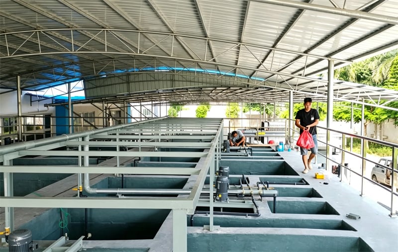
Wastewater generated from Silicon Carbide (SiC) and Gallium Nitride (GaN) semiconductor manufacturing mainly originates from epitaxial growth, etching, ion implantation, thin-film deposition, wafer grinding and cleaning, as well as cleanroom rinsing processes. Compared with conventional silicon semiconductor wastewater, third-generation semiconductor wastewater has a much more complex composition and is significantly more difficult to treat.
Typical contaminants include fluoride, high concentrations of acids and alkalis, ultra-fine silicon carbide particles, gallium compounds, nitrides, trace heavy metal ions, and small amounts of organic contaminants such as photoresist residues and stripping chemicals, resulting in fluctuating COD levels.
The wastewater is characterized by alternating strong acidic and alkaline streams, high fluoride concentrations, ultra-fine suspended solids, and highly corrosive properties. Stable colloidal particles settle very slowly, increasing the risk of pipeline fouling and membrane blockage. In addition, wide-bandgap semiconductor manufacturing requires ultra-high-purity reclaimed water, with water quality standards that are considerably stricter than those of conventional industrial wastewater treatment.
Manufacturers of SiC and GaN semiconductors commonly face several wastewater treatment challenges.
Ultra-fine SiC and GaN particles are difficult to remove through conventional sedimentation, resulting in sludge accumulation, equipment blockage, frequent membrane fouling, and costly production downtime. High-fluoride wastewater generated during etching processes is difficult to treat consistently, making compliance with increasingly stringent environmental discharge standards challenging.
The production process also generates alternating acidic and alkaline wastewater streams with high corrosiveness, requiring specialized corrosion-resistant equipment rather than standard industrial systems. At the same time, semiconductor manufacturers demand extremely high ultrapure water recovery rates, while conventional treatment technologies often fail to meet the required water quality, leading to excessive freshwater consumption and higher operating costs.
Furthermore, modern semiconductor fabs typically have limited installation space and rapidly evolving production lines, making conventional large-scale treatment facilities difficult to expand or upgrade. As a result, there is growing demand for compact, modular, and fully customized wastewater treatment systems designed specifically for high-precision semiconductor manufacturing.
To address the high fluoride content, ultra-fine particles, and corrosive characteristics of SiC and GaN wastewater, we employ a dedicated treatment process consisting of:
Segregated Collection → Precision pH Adjustment & Colloid Destabilization → Coagulation & Fluoride Removal → Fine Filtration → Advanced Membrane Purification → Ultrapure Water Reuse
Acidic, alkaline, fluoride-containing, and process wastewater streams are collected and equalized separately to minimize hydraulic and water quality fluctuations. Precision pH control destabilizes colloidal particles, while an optimized coagulation and sedimentation system efficiently removes suspended solids and the majority of fluoride.
Activated carbon adsorption and precision filtration eliminate trace organic compounds and residual metal contaminants. The treated water then passes through an Ultrafiltration (UF) system followed by an anti-fouling Reverse Osmosis (RO) system for deep desalination, producing high-purity water suitable for wafer cleaning and other semiconductor manufacturing processes.
Core equipment includes:
This solution is specifically engineered for third-generation SiC and GaN semiconductor manufacturing, effectively addressing three critical industry challenges: ultra-fine particle removal, fluoride control, and corrosion resistance.
The treated water consistently meets both production reuse requirements and environmental discharge standards. Customized non-standard equipment can be designed to accommodate compact plant layouts and highly corrosive operating environments, featuring reinforced anti-corrosion structures, anti-clog flow channels, and modular compact designs tailored to semiconductor facilities.
All core electrical control systems, mechanical equipment, and water treatment components are manufactured in compliance with internationally recognized CE, UL, and ISO standards, ensuring superior safety, reliability, and regulatory compliance for high-end semiconductor applications.
The system offers excellent resistance to water quality fluctuations, significantly reducing membrane fouling, maintenance frequency, and operational downtime. Water reuse rates can exceed 95%, substantially reducing freshwater consumption and overall operating costs.
Its modular, space-saving design enables flexible capacity expansion, while fully automated intelligent control ensures stable operation for continuous, high-precision semiconductor manufacturing.
We have successfully delivered wastewater treatment systems for SiC and GaN semiconductor wafer manufacturing facilities, including a benchmark wide-bandgap semiconductor production plant with a treatment capacity of 900 m³/day.
The system has operated reliably, effectively eliminating particle accumulation, stabilizing fluoride removal, and consistently producing reclaimed water that meets semiconductor ultrapure water reuse requirements. The project successfully passed both factory acceptance testing and environmental compliance inspections.
Supporting documentation includes:
We provide comprehensive EPC turnkey wastewater treatment solutions for third-generation semiconductor manufacturers, covering site investigation, water quality analysis, customized process engineering, non-standard equipment manufacturing, installation, commissioning, operation & maintenance services, system upgrades, and lifetime consumables supply.

 EN