
semiconductor-wafer-fab-wastewater-treatment-solution, semiconductor-wafer-fab-wastewater-treatment-solution, /solutions
EN
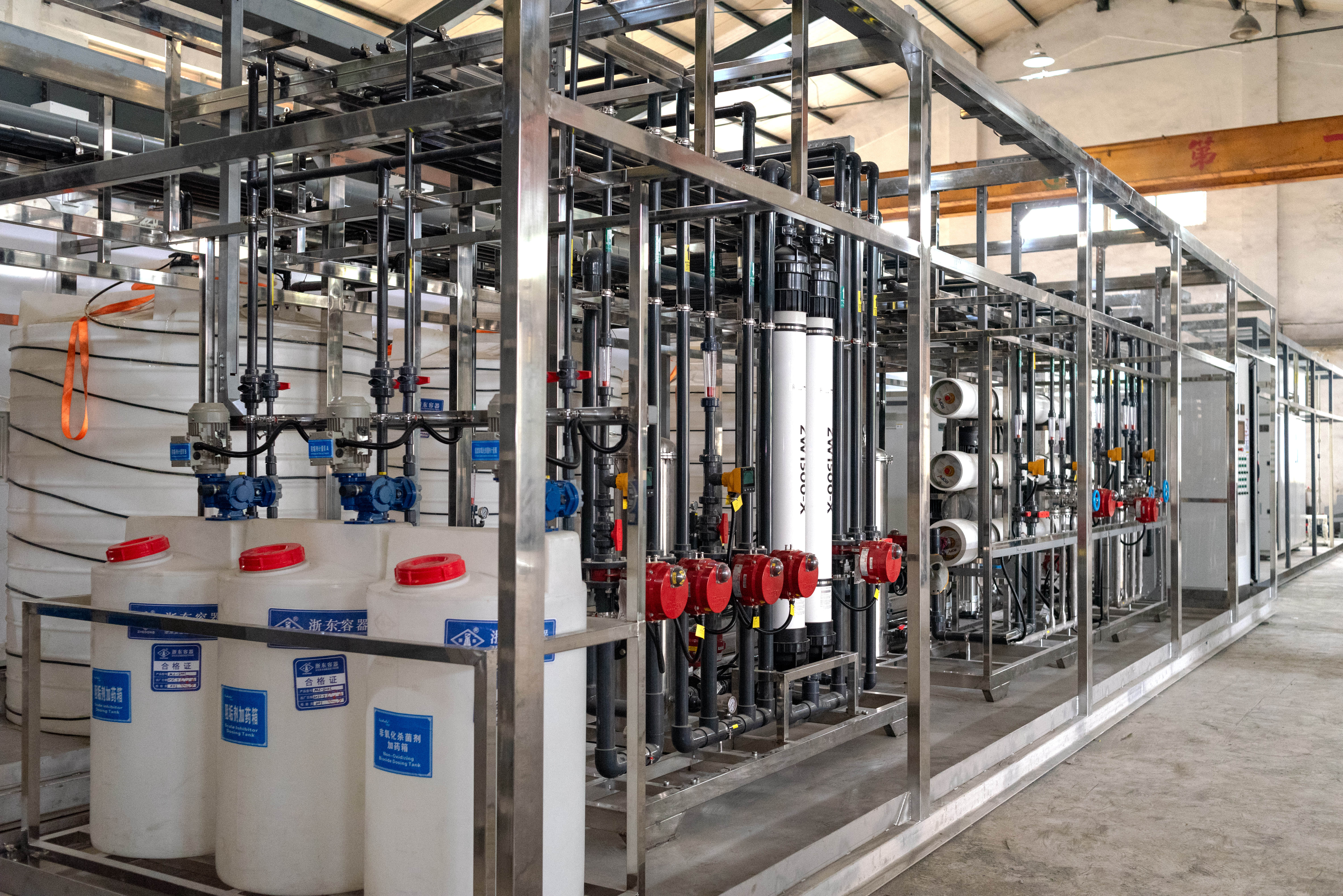
Wastewater generated from semiconductor wafer fabrication (Wafer Fab) is highly complex and consists of multiple process streams. It is primarily generated during wafer etching, thin-film deposition, ion implantation, photolithography, chemical mechanical planarization (CMP), acid and alkaline cleaning, and exhaust gas scrubbing. These wastewater streams are generally classified into five categories: fluoride-containing wastewater, acidic and alkaline wastewater, organic wastewater, heavy metal wastewater, and high-salinity concentrate.
Typical contaminants include fluorides, silicates, boron and phosphorus compounds, trace heavy metals (such as copper, nickel, and zinc), photoresist residues, organic solvents, surfactants, ultrafine suspended particles, and colloidal impurities.
Semiconductor wafer fab wastewater is characterized by significant fluctuations in flow rate, alternating acidic and alkaline conditions, highly stable colloidal particles, poor biodegradability, and a high potential for scaling and corrosion. Some heavy metals exist as stable metal complexes that are difficult to remove using conventional treatment methods.
In addition, semiconductor manufacturing facilities are subject to extremely stringent environmental discharge and water reuse standards, making wafer fab wastewater one of the most technically challenging industrial wastewater streams to treat.
Wastewater treatment in semiconductor wafer fabrication presents several highly specialized technical challenges.
Complexed heavy metals and stable fluoride-silicate compounds are difficult to remove using conventional treatment processes, making compliance with increasingly stringent discharge standards difficult when wastewater characteristics fluctuate.
Ultrafine colloidal particles and photoresist residues frequently cause sludge accumulation, pipeline blockage, and severe membrane fouling, resulting in frequent equipment shutdowns that interrupt continuous wafer production.
Because semiconductor fabrication involves numerous manufacturing processes producing different wastewater streams, combined treatment often requires excessive chemical dosing and generates large volumes of sludge, leading to high operating and disposal costs.
Standard wastewater treatment equipment generally lacks the corrosion resistance, anti-fouling capability, and cleanliness required for semiconductor manufacturing, increasing the risk of secondary contamination.
Furthermore, semiconductor fabs continuously expand production capacity while maintaining compact cleanroom layouts. Conventional civil wastewater treatment facilities occupy large footprints and provide limited flexibility for future expansion, creating demand for fully integrated and customized wastewater treatment solutions.
To address the diverse and technically demanding characteristics of semiconductor wafer fab wastewater, we utilize a fully integrated treatment process consisting of:
Segregated Collection → Decomplexation & Water Conditioning → Fluoride & Silica Removal → Coagulation & Sedimentation → Biological Treatment → Advanced Membrane Purification → Concentrate Volume Reduction
Individual wastewater streams are collected and equalized separately to minimize hydraulic and water quality fluctuations.
A dedicated decomplexation process breaks down stable heavy metal complexes before a precision fluoride and silica removal system selectively removes characteristic contaminants.
The wastewater then undergoes coagulation and sedimentation, followed by advanced oxidation to degrade refractory organic compounds.
A biological treatment system further removes residual COD before the water passes through an Ultrafiltration (UF) system and an anti-fouling Reverse Osmosis (RO) membrane system for advanced purification.
High-quality reclaimed water is reused in semiconductor production cleaning processes, while concentrated wastewater undergoes further volume reduction for efficient disposal and resource recovery.
Core equipment includes:
This solution is specifically engineered to address the complex wastewater conditions encountered in semiconductor wafer fabrication facilities.
The proprietary treatment process effectively removes heavy metals, fluoride-silicate compounds, and refractory organic contaminants while consistently producing treated water that satisfies both environmental discharge regulations and plant water reuse requirements.
We provide fully customized equipment solutions based on cleanroom layout, wastewater characteristics, production capacity, and available installation space. Customized corrosion-resistant equipment housings, wear-resistant materials, anti-clog flow channels, and compact modular equipment ensure optimal performance under demanding semiconductor operating conditions.
All core equipment, electrical control components, and water treatment systems are certified to CE, UL, and ISO standards, meeting the stringent safety and compliance requirements of advanced semiconductor manufacturing facilities worldwide.
The segregated treatment process provides excellent resistance to hydraulic and water quality fluctuations, significantly reducing maintenance frequency, membrane fouling, and sludge generation.
Water recovery rates exceed 95%, substantially reducing freshwater consumption and operating costs while improving overall production efficiency.
The modular integrated design minimizes installation space, allows flexible future expansion, and supports fully automated operation for continuous, high-volume semiconductor manufacturing.
We have successfully completed wastewater treatment projects for multiple 12-inch and 8-inch semiconductor wafer fabrication facilities.
A representative project is a Comprehensive Wastewater Treatment & Water Reuse System for an Advanced Wafer Fabrication Facility, with a treatment capacity of 1,200 m³/day.
The system has demonstrated long-term stable operation, successfully resolving issues related to excessive fluoride and silica concentrations, residual heavy metals, and membrane fouling. The project passed both environmental acceptance inspections and stringent factory water quality verification, ensuring stable wafer production and continuous manufacturing operations.
Supporting documentation includes:
We provide comprehensive EPC turnkey wastewater treatment solutions for semiconductor wafer fabrication facilities, including site investigation, wastewater sampling and analysis, customized process engineering, non-standard equipment design, manufacturing, installation, commissioning, operation and maintenance services, system upgrades, and lifetime consumables supply.

 EN